Electron Beam Evaporation Coating Equipment
High-purity evaporation for precision optical and semiconductor films
System Overview
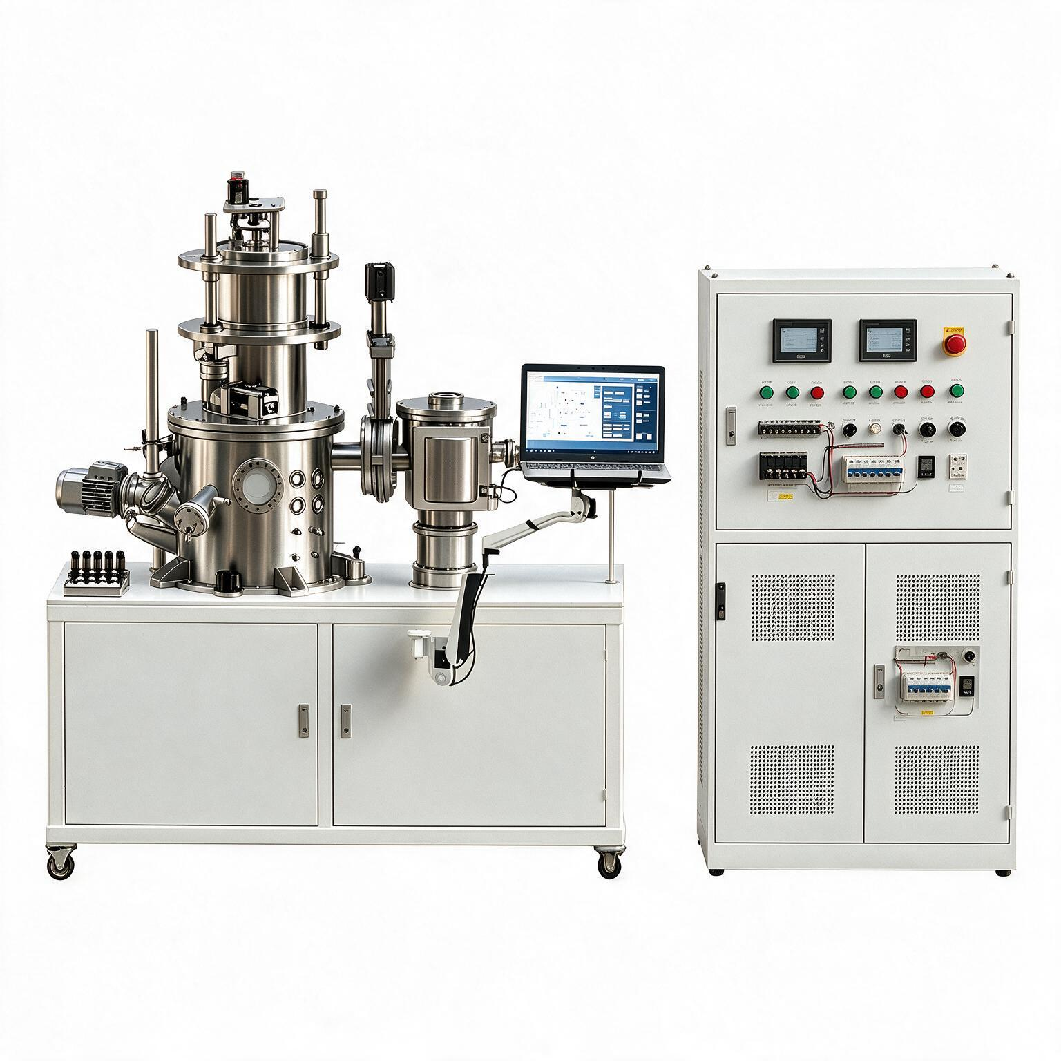
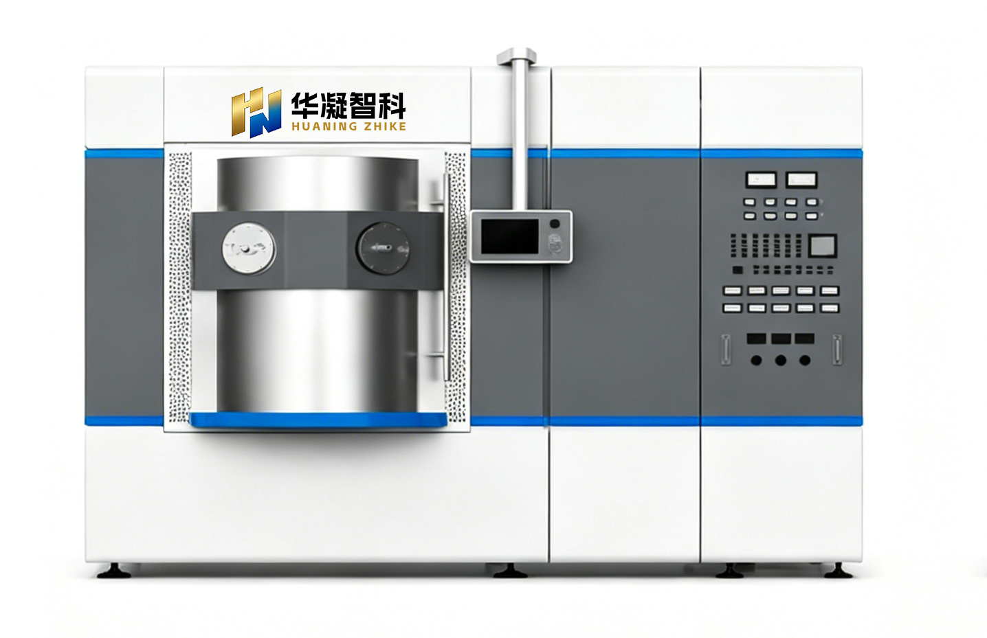
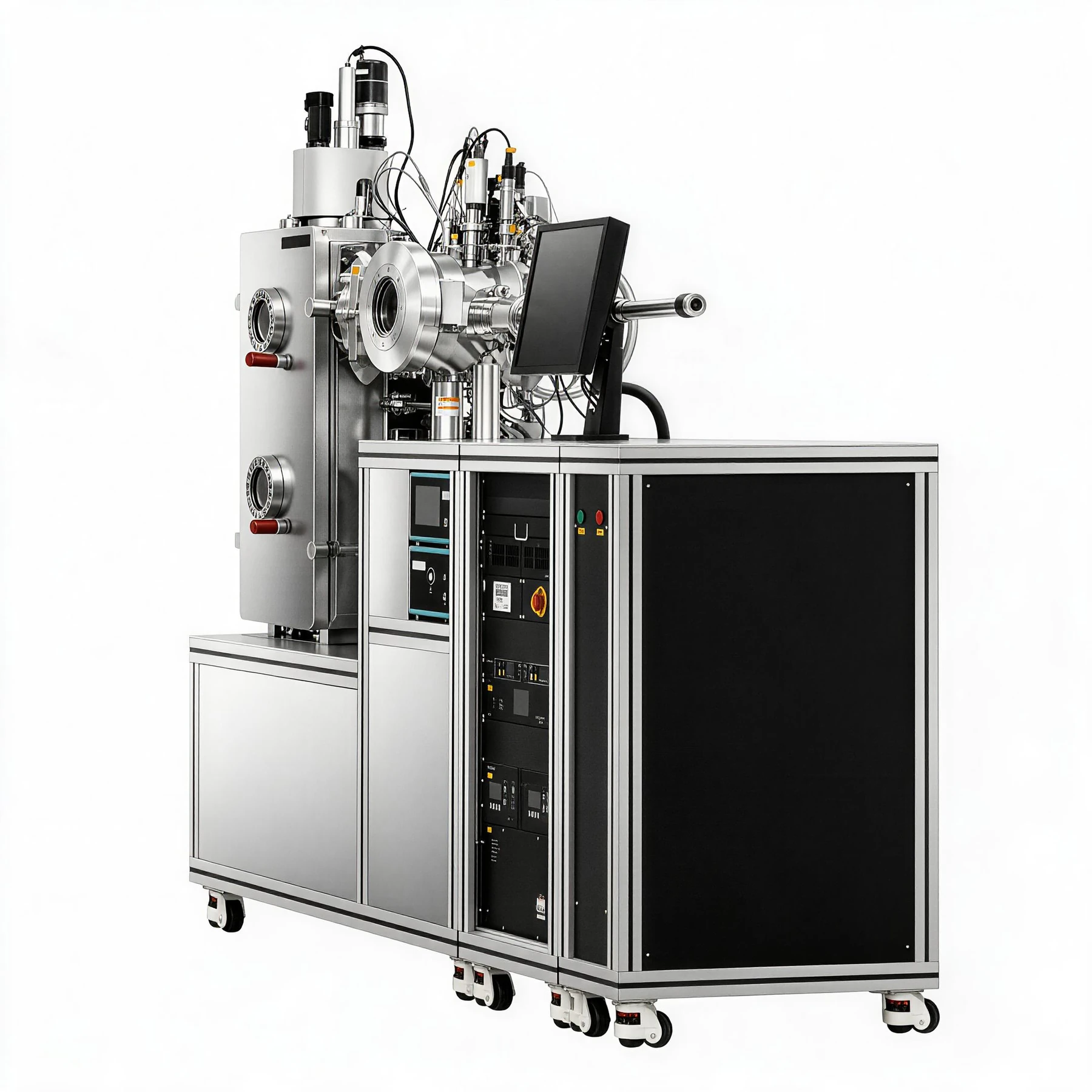
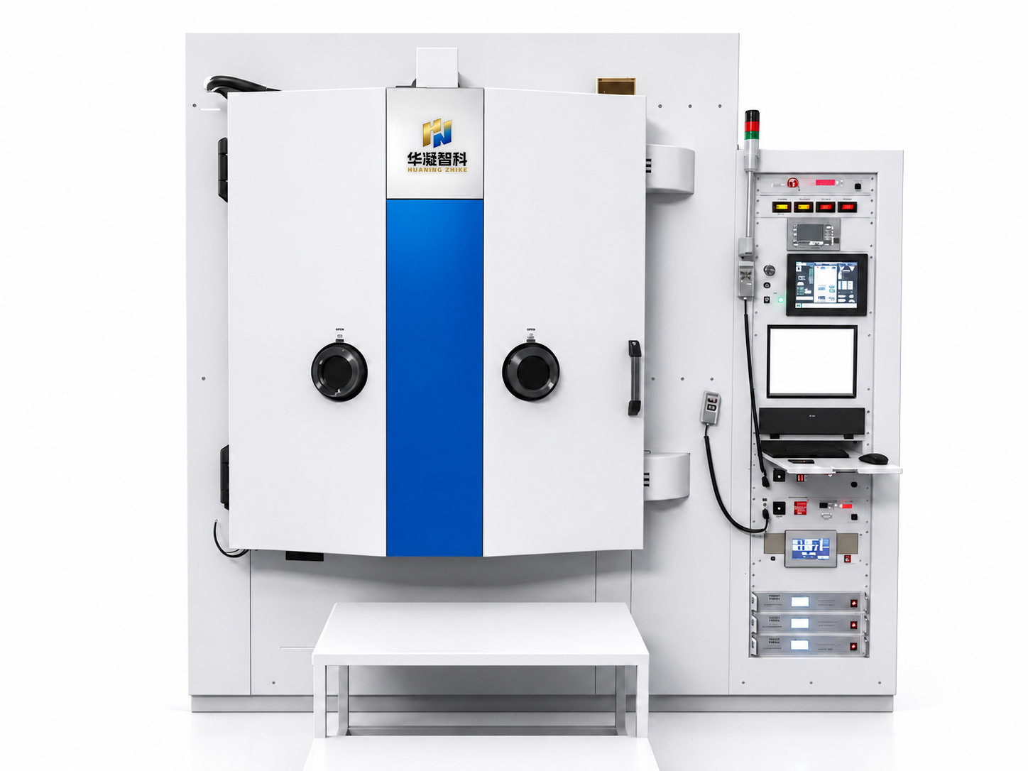
The HN-EB-004 electron beam evaporation system is engineered for deposition of high-purity, low-contamination thin films on optical components, semiconductor substrates, and precision devices. The focused electron beam delivers precise thermal energy to the source material, enabling evaporation of refractory metals and high-melting-point oxides with excellent film stoichiometry control.
Working Principle
A high-energy electron beam — generated by a heated filament cathode and accelerated to kilovolt-range energies — is magnetically deflected onto a target material held in a cooled copper hearth. The concentrated energy evaporates the source material, creating a directional vapor flux that condenses on substrates positioned above. Configured ion-beam-assisted deposition improves film density and adhesion without elevating substrate temperature.
Core Advantages
- High-purity evaporation with minimal source contamination
- Compatible with refractory metals, SiO₂, TiO₂, Ta₂O₅, MgF₂, and more
- Multi-pocket rotating hearth for sequential material deposition
- Ion-beam-assisted deposition for dense, low-stress films at low substrate temperature
- Crystal oscillator in-situ thickness and rate control
- Large-area planetary substrate fixture for optical coating uniformity
- Clean UHV-compatible chamber design
Technical Specifications
| Chamber | Optical-grade highly polished vacuum chamber |
|---|---|
| Evaporation Source | 8 kW, 4-crucible, 270° deflection electron-beam gun |
| Vacuum System | Turbomolecular and titanium-pump system; ultimate pressure 3 × 10⁻⁵ Pa |
| Workpiece Fixture | Multi-axis planetary rotation fixture |
| Temperature Control | Segmented infrared precision heating |
| Ion Assistance | Ion-beam-assisted deposition for enhanced film density and adhesion |
| Monitoring | Online optical monitor with automatic multilayer endpoint detection |
Specifications are representative. Final system parameters are defined during configuration. Contact our engineering team for detailed documentation.